By Joseph F. Krause, co-founder and CEO, Radical AI
The next great semiconductor breakthrough will come down to new materials, not just engineering.
The field is running into multiple walls of physics: the minimum wavelength of visible light, carrying current with less than an electron, electrical insulators with high thermal transport.
As linewidths shrink below 2 nanometers, engineers are hitting quantum tunneling limits, atomic-scale interface effects, and thermal budgets that the classical semiconductor materials can’t handle.
Copper interconnects “feel” the interface just a few nanometers away. Thin-film resistivity in a 5-nanometer interconnect is ten times higher than its bulk value.
New materials are critical to implementing new device and chip architectures to get around these walls of physics. Just as HfO2 enabled a new transistor early in the new millennium, today we need new materials to replace copper, enable the heat transport for GPU high-bandwidth memory, and more.
Semiconductors are clearly the future, but the methods for finding new semiconductor materials are stuck in the past.
Discovery still runs the way it has for decades: A scientist reads the literature, forms a hypothesis, synthesizes a candidate, characterizes it, waits, and starts the next iteration weeks later. It’s a linear, one-step-at-a-time practice.
Considering the multiple property requirement axes a modern interconnect, dielectric, or packaging material has to satisfy simultaneously, it’s easy to see why the path from lab discovery to a qualified, new material in a selling product usually still runs 10 to 20 years.
These multi-dimensional and multi-step bottlenecks are exactly the types of problems robotics and automation can now solve. The industry has focused its automation at the yield, defect, and process optimization level, and is now remarkably good at the production level.
The materials discovery and screening step that determines what goes into the fab in the first place has barely been touched. And some who have attempted it have failed so spectacularly that they’ve spooked the rest of the industry.
The companies that stay scared will quickly find themselves far behind the first movers.
Automation is not the same as self-driving
There’s an important distinction between an automated lab and a self-driving lab. Automated labs offer cruise control. A self-driving lab is more like a Waymo.
An automated lab still requires a person to decide what to synthesize, what to test, and how to interpret the result. It just executes those steps faster.
In a self-driving lab, you specify the property target(s) (e.g. resistivity, a defect-free interface, a hafnium-free dielectric with equivalent performance) and then the system finds its own path there.
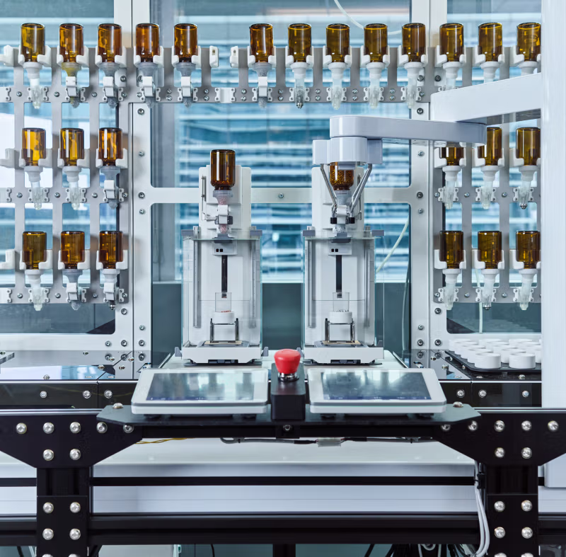
Scientific agents read the literature, generate and rank hypotheses, and run atomic-level simulations that refine and expand the considered compositions. The agents send candidates directly into a physical lab for synthesis and characterization.
Robotic systems enable automatically stepping through the sample handling and instrumentation. The results feed back into the next round of agent hypotheses automatically in a closed loop that runs around the clock instead of one experiment at a time.
It’s imperative to understand the importance of a physical lab generating real experimental data. Simulation alone also isn’t the ground truth.
A model without a physical execution layer still misses how a material actually behaves once it’s synthesized, tested, and integrated. That physical validation step is what makes the data trustworthy enough to build a fab process around.
This isn’t a hypothetical. Systems like this are running today, producing hundreds of novel material compositions in weeks rather than years, with the most promising candidates sent out for independent third-party verification.
The capability exists. We’ve demonstrated properties for a new material that beats one of the most important materials in structural and aerospace applications. The question now is how quickly the semiconductor industry adopts it, as the ones who do will have a big advantage over those who don’t.
Where this hits first
The nearest-term opportunities sit where the walls of physics are already staring us in the face: interconnects, high-k gate materials stacks, and packaging materials.
Interconnects, because resistivity scaling at sub-10-nanometer linewidths is now dominated by surface and grain-boundary effects that bulk-material data simply doesn’t capture.
High-k gate stacks, because Hafnium was one of the original material advances in the industry, but is now over 20 years old.
Due to supply constraints in a handful of countries, the price has risen roughly tenfold over the past four years, exposing every advanced node to geopolitical risk.
Finally, the walls of physics are pushing packaging into heterogeneous, 3D-stacked architectures that demand thermal interface materials, contact metals, and low-k dielectrics that weren’t originally designed and selected for this use case.
None of these are single-property optimization problems. A packaging material has to hit mechanical, thermal, electrical, and adhesion targets simultaneously – exactly the type of multi-objective problem that benefits from running hundreds of candidate compositions and process conditions in parallel instead of one at a time.
Concurrent engineering, not sequential engineering
The deeper shift this enables is concurrent engineering: designing the material and the product at the same time, instead of designing the product around whatever materials are already qualified.
Charles Kuehmann, SpaceX’s VP of Materials, has spoken publicly about this as a key unlock for rapid iteration in aerospace. Semiconductor R&D isn’t there yet, but it needs to be.
Today, product engineers choose packaging, substrate, and interconnect strategies constrained by a materials menu that has marginally expanded in a generation, largely because discovery took too long to be part of the conversation.
When materials discovery runs in weeks instead of years, it goes from being a roadmap constraint to an accelerant.
I felt this firsthand in my PhD work, synthesizing novel 2D materials for neuromorphic chips at the US Army Research Lab. Unfortunately, the slow and fragmented nature of this “sequential engineering” prevented any new materials from ever reaching a test chip.
It’s important to be clear about what this does and doesn’t solve. Delivering a finished chip involves supply chain, defect, and yield challenges that autonomous materials discovery doesn’t address on its own.
A national competitiveness question, not just a technical one
The materials research stage underpinning the semiconductor materials stack development has been the slowest-moving stage for a long time. But it’s a gap we have the technology to close now.
Countries that figure out how to compress materials discovery from decades to months won’t just move faster on next-generation chips: they’ll be less exposed to supply chains they don’t control, and less constrained by materials whose replacements should have arrived years ago.
For an industry built on the premise that the next generation always arrives faster than the last, it’s worth asking why materials discovery – the thing everything else depends on – has been allowed to move so slowly for so long.
Robotics and automation solved this problem for production years ago. It’s time they solved it for discovery, too.

About the author: Joseph F. Krause is co-founder and CEO of Radical AI, a materials technology company using AI and autonomous laboratories to accelerate the discovery of advanced materials.
