Vexlum, a manufacturer of advanced semiconductor lasers for high-impact applications, has announced it has secured €10 million in funding to scale its proprietary semiconductor chip manufacturing and laser technology operations in Finland.
The round consists of €6 million in equity investment led by Kvanted, with participation from Finnish state-owned Tesi (Finnish Industry Investment Ltd) and the EIC Fund, alongside a €2.4 million grant from the EIC Accelerator, and a €1.6 million loan from Nordea.
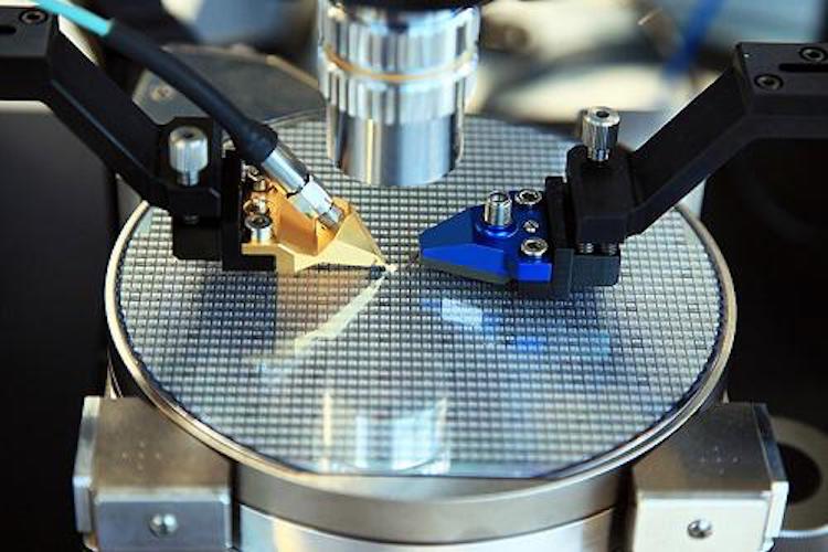
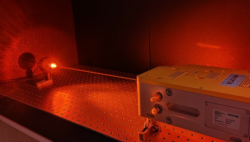
Vexlum’s semiconductor-based Vertical-External-Cavity Surface-Emitting Laser (VECSEL) technology addresses a critical bottleneck in high-tech industries: the lack of compact, cost-effective, high-power laser sources at precise wavelengths. [Read more…] about Vexlum raises €10 million to scale semiconductor and laser manufacturing