
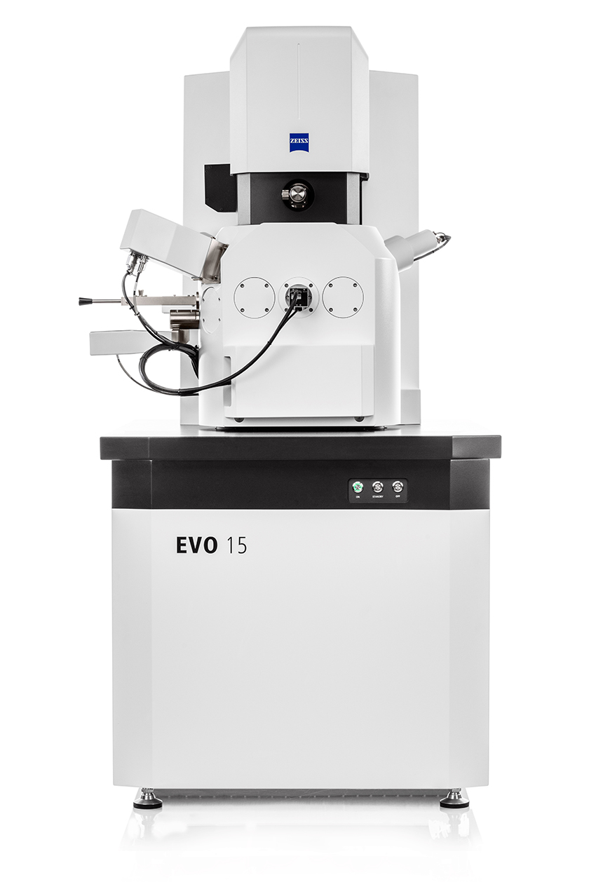
Zeiss, which claims most of the world’s microchips are manufactured using its optical technologies, has launched the new generation of its scanning electron microscope system.
The company says the new instruments in the Zeiss EVO product family feature various improvements in terms of usability, image quality and seamless integration into multimodal work processes.
With the variety of options available, the Zeiss EVO family of devices can be precisely tailored to life science, materials science or routine industrial quality assurance requirements.
Zeiss says EVO delivers high-quality data even under difficult conditions.
For example, when non-conductive parts need to remain unprepared for transfer from one instrument to another during industrial quality assurance or samples such as pollen to be classified should be imaged in their naturally hydrogenated state.
For these requirements ZEISS EVO offers various vacuum modes, such as high vacuum, variable pressure and high pressure as well as different detector technologies – SE, C2D, C2DX, BSE, EDS.
An optional lanthanum hexaboride emitter produces a brighter electron beam for better image resolution and noise reduction.
The “intuitive, user-friendly handling” makes Zeiss EVO suitable for both trained and inexperienced microscope users, claims the company.
Jim Suth, quality manager at ECR Engines, says: “Zeiss SmartSEM Touch is an extremely simplified user interface designed specifically for the occasional operator who has “little or no experience with SEMs”, such as in central microscopy laboratories or laboratories for industrial quality assurance.
“The new Zeiss SmartSEM Touch user interface from Zeiss EVO is so clear that not only trained microscopists, but also our technicians and interns without REM knowledge can learn how to handle them in 20 minutes.
“The system’s imaging and analysis capabilities are a great advantage. The seamless integration into multimodal work processes makes our work much more efficient.”
The US-based ECR specializes in the production, research and development of high-performance engines and uses Zeiss EVO for material characterization and fault analysis.
SEM material characterization for academic or industrial purposes is part of a work process in many environments where samples are examined using other imaging or analytical technologies such as light microscopes or spectrometers.
Zeiss says EVO can be configured as part of a semi-automated, multimodal workflow because it has tools that “seamlessly locate interesting regions and ensure the integrity of data across multiple processes”.
In such configurations, Zeiss says EVO enables highly productive correlative microscopy and analysis methods that provide users with more meaningful data and a deeper understanding of their samples.