You might find old electronic products that are not supported anymore. If you reverse engineer circuit board parts from these, you can fix and improve them. Many people do this to repair old gadgets or make them last longer.
Some want to avoid planned obsolescence. Sometimes, you need to reverse engineer circuit board layouts if you cannot find schematics or repair guides.
People reverse engineer circuit board components for different reasons:
- To replace old boards in discontinued electronic products
- To rebuild schematics from hardware in discontinued electronic products
- To make working replacements for discontinued electronic products
You can also use IC decryption to unlock chips. This helps you take care of old systems. If you learn PCB reverse engineering, you can keep old electronic products working for many years.
Key Takeaways
- PCB reverse engineering lets you fix old electronics. You can make new schematics and keep devices working longer.
- Use a clear step-by-step process for reverse engineering. List all parts, take pictures of the PCB, and copy the layout to be accurate.
- Use the right tools for good PCB analysis. Digital multimeters and X-ray inspection help you get important data.
- Know the legal and ethical rules for PCB reverse engineering. Always ask for permission and respect original designs to avoid trouble.
- IC unlock techniques can get useful data from chips. Use direct readout or glitching attacks to get information safely.
PCB Reverse Engineering Basics
What is PCB Reverse Engineering
PCB reverse engineering helps you figure out how a circuit board works. You start with a finished pcb and try to make a schematic. This lets you see how parts connect and how signals move.
Printed circuit board reverse engineering means you take apart a pcb to learn about its design. You can make new documents or improve the board.
PCB reverse engineering is not the same as PCB copy and IC unlock. PCB reverse engineering looks at the board and its connections. You check how parts link and how signals travel. IC decryption is about unlocking the code inside a chip. You want to copy or study the program data in the chip.
When you reverse engineer a pcb, you often rebuild the schematic. This shows how each part works with others. You use the schematic for repairs, upgrades, or making new boards. It also helps you find problems if something breaks.
Tip: Set clear goals before you start. Decide if you want to fix, upgrade, or just learn about the pcb. This will help you collect the right data.
Key Steps to Reverse Engineer Circuit Board
There is a simple path for pcb reverse engineering. Each step helps you gather data and build a schematic. Here are the main steps:
- Cataloging Components: Write down every part on the pcb. Make a Bill of Materials (BOM) list. This helps you find parts and build the schematic.
- Removing Components (If Needed): Take off parts carefully if you need to see traces or test them. Keep track of where each part goes.
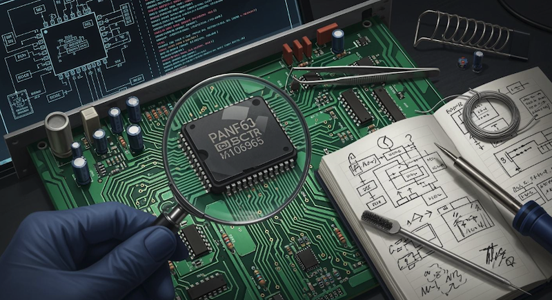
- Photographing and Scanning the PCB: Take clear pictures of both sides of the pcb. These photos help you map out traces and connections.
- Image Correction and Trace Mapping: Edit your photos to make traces easier to see. This helps you draw the schematic.
- Identifying Pads, Traces, and Vias: Mark every pad, trace, and via. This step helps you find parts and see how signals move.
- Aligning and Layering Images for Double-Sided Boards: Line up images from both sides. This helps you see how traces connect through the board.
- Recreating the PCB Layout in Design Software: Use software to draw the board. You can make a new schematic and files for a new pcb.
- Creating a Bill of Materials (BOM): List all parts and their details. This helps with repairs and future analysis.
- Testing and Troubleshooting: Check your work. Test the board and look for problems. Use failure analysis if something does not work.
For multi-layer boards, you repeat some steps. You scan or image each layer. This gives you all the data you need for a full schematic and analysis.
Note: If you skip steps or miss data, you may have trouble finding signals or parts later.
Tools and Imaging Techniques
You need the right tools for pcb reverse engineering. Some tools help you find parts, others help you collect data or build the schematic. Here are some common tools:
- Digital Multimeter (DMM): Measures voltage, current, and resistance. You use it for quick checks and signals.
- SMD LCR Meter: Measures small parts like capacitors and resistors. It helps you find parts.
- Power Supply: Lets you test the pcb and see how it handles signals.
- Universal Device Programmer: Programs chips and helps with deeper data analysis.
- Multi-Protocol Adapter: Talks to different chips and helps with data collection.
For imaging, you have many choices. Some work better for single-layer boards, others are best for multi-layer boards. Here is a table of common imaging techniques:
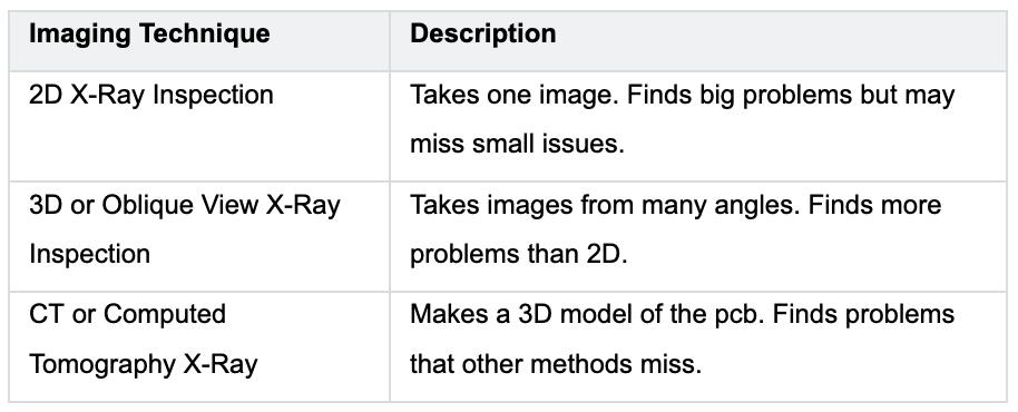
X-ray systems let you see inside a pcb without taking it apart. These systems find problems like bad solder joints or misaligned parts. They can see tiny gaps as small as 10 micrometers.
Modern pcb reverse engineering uses new techniques. Automated Optical Inspection (AOI) uses cameras and AI to find parts and traces. 3D X-ray CT makes detailed models of the inside of a pcb. Electromagnetic Field Analysis lets you study signals and data without opening the board. These tools help you collect better data and make a more accurate schematic.
Alert: Always check your schematic and data before making a new pcb. Mistakes in finding parts or signals can cause problems later.
You should know the best ways for single-layer and multi-layer boards. For single-layer boards, you can often see all traces and pads. For multi-layer boards, you need imaging or careful delamination.
Always keep your data organized. Use clear labels for every part and signal. This helps with schematic work and finding problems.
If you follow these steps and use the right tools, you can do pcb reverse engineering well. You will get a clear schematic, good data, and a working board.
PCB Copy and Clone
What is PCB Copy vs. PCB Clone
You may hear people use the terms pcb copy and pcb clone. These words sound similar, but they have different meanings in pcb reverse engineering. When you copy a pcb, you make an exact replica of the original board.
You use pcb reverse engineering to match the layout, parts, and connections. Cloning a pcb goes further. You can copy the board, but you may also change or improve the design. Cloning lets you add new features or fix old problems. Both methods help you save time and money by using existing data instead of starting from scratch.
Step-by-Step Process for PCB Copying
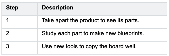
You can follow a clear process to copy a pcb. Each step helps you collect data and rebuild the board:
- Preparation: Clean the pcb and remove any coatings. Take out components so you can see all traces and pads. This step helps you get good data for the next steps.
- Schematic Generation: Trace all connections and identify each part. Use pcb reverse engineering to create a digital schematic. This schematic shows how signals move and how parts connect.
- PCB Layout Reconstruction: Place each part in the right spot. Draw all traces and check your work. Use design software to make sure your data matches the original pcb.
- Bill of Materials (BOM) Creation: List every part and its details. This data helps you find and buy the right components for your new pcb.
Key Considerations and Quality Control
You need to check your work at every step. Good quality control keeps your pcb working well. Use this table to guide your checks:
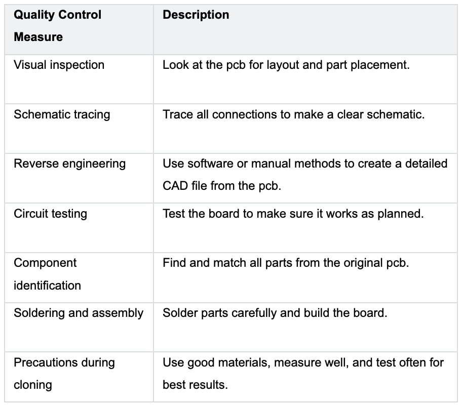
Tip: Always double-check your data and connections. Use high-quality tools and materials. Test your cloned pcb with the original device to make sure it works.
Typical Applications and Limitations
You use pcb reverse engineering to copy or clone boards for many reasons. You can keep old machines running when you cannot buy new parts.
You can use pcb reverse engineering to rebuild lost data or restore a design when the maker stops making the product. Many people use pcb reverse engineering to fix industrial control systems or other important equipment.
You may face some limits. Complex boards with many layers or hidden parts can make pcb reverse engineering hard. If you use poor parts, your pcb may not work well.
You must test your data and board to avoid problems. Copying or cloning a pcb without permission can break the law, so always check before you start.
IC Unlock and Decryption
Advanced IC Unlock
Sometimes, you want to find out what is inside an ic. This helps you learn how the ic works and stores data. You use IC unlock to fix, copy, or make old electronics better. Many people use IC decryption with pcb reverse engineering and iwm reverse engineering to keep devices working.
There are different ways to study an ic. These methods help you get the layout and find hidden data. The table below shows some good techniques:
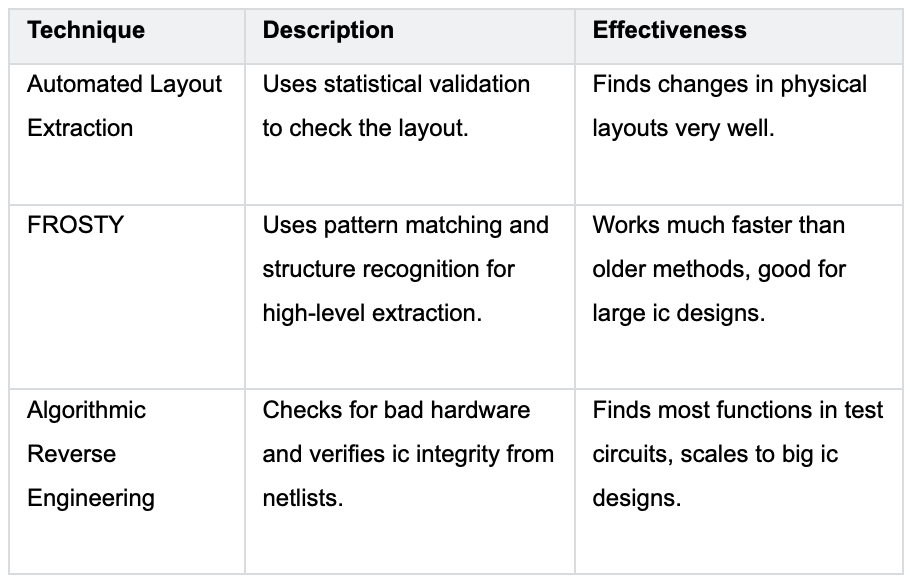
These techniques help you see the ic clearly. Automated layout extraction helps you spot errors in the chip. FROSTY lets you work fast, even with big ic layouts.
Algorithmic reverse engineering helps you find hidden problems or extra circuits. If you use these with pcb reverse engineering and iwm reverse engineering, you can understand the whole device.
Tip: Keep your data neat and organized. Good notes help you match ic layouts with pcb traces and iwm reverse engineering results.
MCU Unlocking Methods
Microcontroller units (MCUs) control how a pcb works. You may need to unlock an mcu to get the data inside. This step is important for iwm reverse engineering and pcb reverse engineering. There are several ways to unlock an mcu:
- Direct Readout: You use a programmer to read the ic directly. This works if the ic does not have strong security.
- Glitching Attacks: You send special signals to the ic to make it skip security checks. This method can help you get the data if the ic has basic protection.
- Decapsulation: You remove the top of the ic and use a microscope to see the data stored inside. This method is slow but works for some chips.
- Side-Channel Attacks: You measure things like power use or temperature changes while the ic runs. These changes can show you the data inside the ic.
- Firmware Extraction: You use special tools to pull the firmware from the ic. This method helps you get the code and data for iwm reverse engineering.
Pick the method that fits your ic and your goal. Some methods work better for simple chips. Others are best for complex or protected ics. Always check your results with pcb reverse engineering and iwm reverse engineering to make sure your data is right.
Note: Some unlocking methods can break the ic. Practice on spare chips before working on rare or important devices.
Challenges and Solutions
You will face many problems when you try ic unlock. Some ics use weak encryption. Attackers can find these weak spots and get the data. Side-channel attacks can also help attackers.
They watch for small changes in power or temperature to find secrets inside the ic. Manufacturing mistakes can make things worse. If companies do not test security well or follow standards, attackers can break into the ic more easily.
You can use some solutions to make ic decryption harder for attackers:
- Use strong cryptographic techniques and hardware security modules. These tools protect the data inside the ic.
- Add code obfuscation. This makes it harder for attackers to use iwm reverse engineering or pcb reverse engineering to find out how the ic works.
- Rotate keys often and use secure enclaves. These steps keep sensitive data safe, even if someone gets into the ic.
Always check your security. Regular testing helps you find weak spots before attackers do. When you use pcb reverse engineering, PCB copy, and ic decryption together, you can keep your devices safe and working.
Alert: Never skip security checks. Good security keeps your data and devices safe from harm.
Motivations for Discontinued Electronic Products
Repair and Restoration
You might want to fix or bring back old electronics that are not made anymore. When you use pcb reverse engineering, you can make these products work again. First, you take apart the pcb and look at each part.
You write down how the parts are set up and connected. This helps you see how the pcb works. After that, you can draw a new schematic and build new boards if you need to. The table below shows how you use pcb reverse engineering for fixing and restoring:
You must collect data at every step. This data helps you find what is broken and swap out bad parts. You also use the data to test the pcb and check if it works like before.
Replication and Enhancement
Sometimes, you want to make a copy of a pcb or make it better. You use pcb reverse engineering to get data from the old board. This data lets you build a new pcb that is just like the old one. You can also use the data to add new things or fix problems.
For example, you might put in better connectors or change the layout to work faster. You need to check your data many times so you do not make mistakes. When you finish, you have a pcb that works well and might be even better than before.
Tip: Always keep your data neat and easy to find. Good notes help you make good copies and easy upgrades.
Innovation and Research
You can use pcb reverse engineering to learn new things and make better products. When you look at old pcb designs, you get data that shows how people solved problems before.
This data helps you learn about old systems and find ways to make them better. You can use the data for research or to build new things. Here are some ways pcb reverse engineering helps with new ideas and research:
- You learn how to fix and upgrade old systems.
- You look at other designs to get new ideas and make your own pcb better.
- You save money and time by using data from old products.
- You work faster by using data and layouts that already work.
You help the electronics world grow when you use pcb reverse engineering. You turn old data into new answers.
Legal & Ethical Issues
Legal Restrictions
You must know the laws before you start pcb reverse engineering. Many countries protect designs with patents and trade secrets. If you copy a pcb without permission, you can break the law. Some laws, like the DMCA, let you reverse engineer for learning or fixing, but you cannot break security features.
You should always check if the pcb design is public or if you have written permission. If you use someone’s data without asking, you can face legal trouble. You must also avoid making fake products that look like the real thing.
Ethical Considerations
You should think about what is right and fair when you work with pcb reverse engineering. If you use data from a pcb, you must respect the work of others. Do not use data to make copies that trick people.
You can use pcb reverse engineering to fix, learn, or improve, but not to steal ideas. Sharing data for learning helps everyone, but selling fake boards hurts trust. You should always tell where your data comes from and give credit when you use someone’s work.
Tip: Ask yourself if your work helps others or just copies someone else’s ideas. Good ethics build trust in the tech world.
Compliance Tips
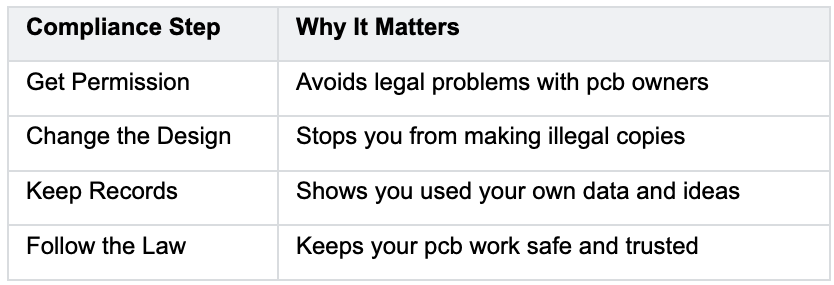
You can follow these steps to stay safe and legal when you use pcb reverse engineering and data:
- Get legal permission or check that the pcb is in the public domain.
- Use pcb reverse engineering to learn or improve, not to make exact copies.
- Keep good records of your scans, tests, and data choices.
- Know the laws in your country, like the DMCA, and do not break security on purpose.
If you follow these steps, you can use pcb reverse engineering and data in a smart and safe way. You protect yourself and respect the work of others.
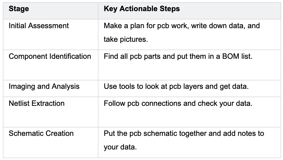
You can do pcb reverse engineering and IC unlock well if you follow simple steps. The table below shows what to do with pcb and data at each step:
You should use good tools, keep your data neat, and act honestly. Some helpful books are The Art of PCB Reverse Engineering, PCB-RE: Tools & Techniques, and PCB-RE: Real-World Examples.
Experts say you should try new things but also follow the law. You can join groups, share pcb data, and learn from other people. Always use pcb reverse engineering in a good way and help others by sharing your data.
FAQ
What is PCB reverse engineering?
You use PCB reverse engineering to study a circuit board. You collect data about parts and connections. This helps you understand how the board works and lets you fix or copy it.
How do you collect data from a discontinued electronic product?
You start by taking clear photos. You write down each part and trace connections. You use tools to scan layers. You organize all data so you can build a new schematic.
Why is data important in IC unlock?
You need data to unlock and study chips. Data shows how the chip stores information. You use data to find weak spots and understand the chip’s functions.
Can you use data to improve old devices?
You can use data from old boards to make upgrades. Data helps you spot problems and add new features. You build better devices by using data from past designs.
What tools help you analyze data in PCB reverse engineering?
You use a multimeter, scanner, and design software. These tools help you collect and check data. You organize data to make schematics and test boards.