The scale and complexity of thin-film deposition in modern manufacturing is extreme. Advanced semiconductor chips can require many deposition steps, creating large stacks of thin-film materials. One of the key inputs behind these processes is the sputtering target.
Sputtering targets are precision materials used inside vacuum chambers in semiconductor manufacturing and other industries, including advanced electronics, photonics, coatings, and displays.
They play an important role in thin-film performance, process stability, and manufacturing consistency, which is why they matter to engineers and production teams.
What is a sputtering target?
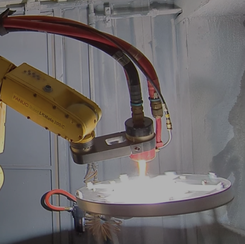
A sputtering target is the source material used in physical vapor deposition, or PVD. In sputtering, ions from a plasma strike the target inside a vacuum chamber and dislodge atoms from its surface. These atoms then travel through the chamber and deposit onto a substrate, forming a controlled thin film.
Depending on the application, sputtering targets can be made from pure metals, alloys, oxides, or other compounds. The selected material depends on the electrical, optical, thermal, or mechanical properties needed in the final film.
Why sputtering targets are important in advanced manufacturing
The sputtering target is not just another consumable. It is a performance-critical input. Material purity, density, grain structure, and uniformity all influence the characteristics of the thin film produced during deposition.
High-purity targets help reduce contamination risk and support more stable sputtering performance. Dense, uniform targets can improve sputter rate consistency, film thickness control, and overall repeatability. In advanced manufacturing, small variations in these properties can affect yield, reliability, and production efficiency.
Thin-film quality matters because these coatings often need to meet strict requirements for conductivity, adhesion, reflectivity, barrier performance, or durability. If the deposited film varies too much in thickness or composition, the final product may not perform as expected.
Where sputtering targets are used
Sputtering targets are used in many thin-film applications, including:
- Semiconductor manufacturing: Copper, aluminum, titanium, and similar materials for conductive films, liners, and barrier layers
- Display: Indium tin oxide and related materials for transparent conductive coatings on glass and electronic displays
- Solar and related fields: Thin films used in photovoltaic structures, transparent conductive layers, and protective coatings
- Medical and optics: Reflective, protective, and functional coatings used in specialized optical and technical applications
- Other industrial wear-resistant surfaces: Thin-film coatings that improve hardness, durability, and resistance to heat or corrosion
What do manufacturers look for in sputter target suppliers
Once thin-film properties are specified, choosing the right sputtering target supplier becomes an important step. Manufacturers usually evaluate suppliers based on purity levels, density, homogeneity, grain size control, dimensional accuracy, and geometry options suited to the application.
For bonded targets, backing plate quality and bond integrity also matter. These factors can affect heat transfer, mechanical stability, fitment, and target performance during operation. In many cases, manufacturers also value suppliers that can support custom specifications and consistent production quality.
Sputtering targets are only one part of a larger manufacturing process, but they have a direct impact on film quality and process consistency. Understanding target performance and selecting the right supplier can help improve production stability and long-term manufacturing results.