Canon launches new semiconductor lithography system
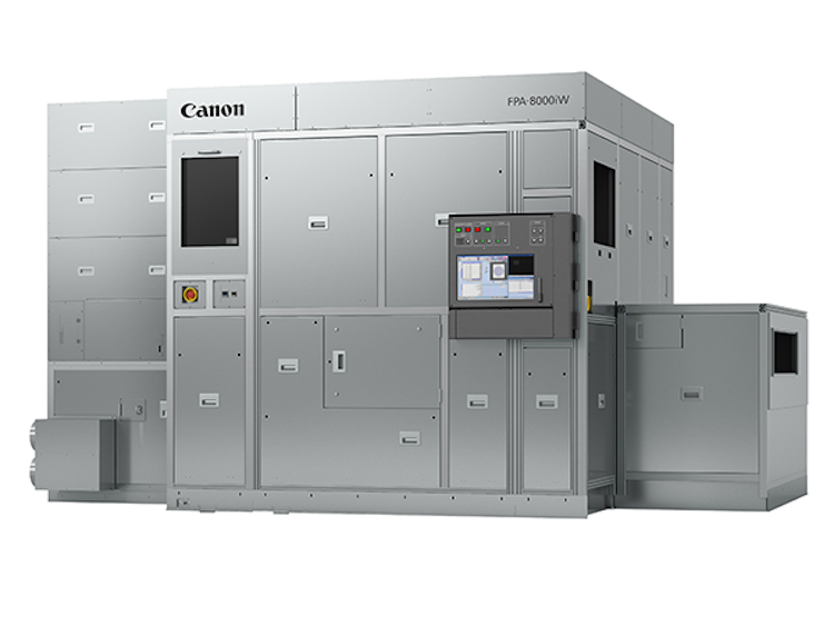
Canon has launched the FPA-8000iW, which it describes as the first Canon semiconductor lithography system to support manufacturing using large panels that are common in back-end processing.
Integrating a proprietary projection optical system, the FPA-8000iW i-line stepper offers a wide exposure field and fine 1 µm† pattern resolution.
The FPA-8000iW was designed to meet the needs of manufacturers aiming for high production efficiency through the use of 515 x 510 mm organic panel substrates for Panel Level Packaging (PLP) applications.
PLP processes typically involve mounting and processing a large number of semiconductor chips on large panels in order to produce packages that can increase communication bandwidth while reducing the power consumption of high-performance computing systems, ideal for such products as CPUs and GPUs utilized by data centers.
Future PLP requirements include cost reduction and further shrinking of semiconductor packaging that protects delicate internal semiconductor circuity from outside environments and electrically connects to external components.
The FPA-8000iW supports PLP cost reduction and package scaling by providing high productivity panel processing with a large exposure field and high resolution.
In response to packaging processes that use panel substrates, Canon developed a new stepper platform capable of handling large 515 x 510 mm panel substrates.
Severe warpage is also common in large panel substrates and the new platform and panel-feeding system can overcome up to 10 mm of panel warpage.
As a result, the FPA-8000iW can help customers realize high-productivity and efficiency for PLP production of large packages.
Canon’s original projection optical system supports a wide 52 x 68 mm exposure field while achieving 1.0 µm resolution. The company claims this is “the finest resolution among packaging exposure systems that support panel substrate processes”.
Canon says these advantages “enable state-of-the-art PLP technology that supports thin substrates with high-integration, enabling flexibility in electronic system design”.