
Kyocera breaks ground on new manufacturing plant
Kyocera has ceremonially broken ground on a new manufacturing plant for ceramic structural components in Kagoshima, Japan.
The new facility will produce durable, high-precision components for semiconductor and LCD manufacturing equipment, says the company.
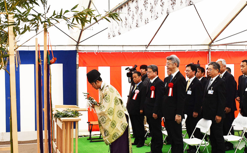
Kyocera held a groundbreaking ceremony last week, attended by the company’s president, Hideo Tanimoto.
Strictly speaking, the new facility is an expansion of the company’s existing manufacturing plant expansion in Kirishima City, Kagoshima, Japan.
The company says it plans to double its production capacity for fine ceramic structural components.

The expansion, scheduled for completion in October 2018, will bring a new building with 29,232 square meters (about 314,650 square feet) of additional space.
The new plant will produce fine ceramic structural components used mainly by companies that manufacture semiconductors or liquid-crystal displays.
Kyocera anticipates rising demand for semiconductors and LCDs as Internet of Things and artificial intelligence applications boost demand for high-speed, high-volume data processing.
The shift from hard-disk data storage to semiconductor memory and solid-state drives has increased demand for semiconductor processing equipment.
Additionally, the proliferation of high-definition display technology in TVs and smartphones has increased demand for the equipment used to manufacture flat-panel displays.
Kyocera’s new plant will produce components used in key manufacturing processes for these and other high-precision products.
Kyocera says its investment will contribute to Kagoshima’s local economy and create employment opportunities.
The groundbreaking is the result of a construction agreement reached in October between Kyocera and the city of Kirishima.
Details of the new plant
- Name: Kyocera Corporation Kagoshima Kokubu Plant #4-1
- Location: On the premises of Kyocera’s existing Kagoshima Kokubu Plant, in Kirishima, Kagoshima, Japan
- Construction cost: Approximately $50.4 million
- Building area: 5,562 sq m
- Total floor space: 29,232 sq m
- Expected start of operations: October 2018
- Main products: Fine ceramic structural components used in semiconductor and flat-panel display manufacturing equipment
- First-year production plan: Approximately $3 million (from October 2018 through March 2019)
Kyocera employs more than 70,000 people worldwide and has annual revenues of around $900 million.