
Sector spotlight: Record growth of semiconductor market good sign for industrial robot manufacturers
The global semiconductor market is growing at a phenomenal rate, evidence of which can be seen by anyone who cares to look around them.
Almost everyone on Earth either directly or indirectly uses some sort of device or machine which contains semiconductor technology.
And in some ways, this is just the beginning of the semiconductor revolution.
As Kawasaki Robotics notes on its website: “In the space of a generation, the semiconductor industry has evolved from a niche specialty to a fundamental driver of the global economy.”
If it’s come this far in so short a time, where will semiconductor technology take us over the next generation?
It’s just too big a question to answer in a short article like this, but what can be said is that the number of semiconductor products in the world will continue to increase and both the products and the semiconductor components themselves will become increasingly sophisticated.
For companies like Kawasaki and other industrial robot makers, such trends almost guarantee ongoing growth in demand for their automation equipment – both from companies which manufacture semiconductors as well as the manufacturers of machines and devices which integrate semiconductors as fundamental components.
To put some numbers on these market trends, we can turn to industry associations such as Semi, which says 2017 was “a terrific year”.
The Europe-based organisation says that chip revenues closed the year at nearly $440 billion, an impressive 22 percent year-over-year growth.
The equipment industry surpassed revenue levels last reached in the year 2000.
Semiconductor manufacturing equipment posted sales of nearly $56 billion and semiconductor materials $48 billion in 2017.
For semiconductor equipment, this was a “giant” 36 percent year-over-year growth, says Semi.
Samsung, alone, invested $26 billion in semiconductor capital expenditure in 2017, which Semi proclaims as “an incredible single-year spend in an incredible year”.
Meanwhile, across the Atlantic in the US, the Semiconductor Industry Association is reporting similarly astronomical numbers.
SIA this week published data showing that worldwide sales of semiconductors reached almost $38 billion for the month of November 2017 alone.
The total for the entire year, says SIA, is likely to go beyond $400 billion.
It’s complicated
According to the international engineering organisation IEEE, the process of making semiconductors is arguably the most complex manufacturing endeavour in the world today.
The reasons for this, says the IEEE, include:
- tightly constrained production processes;
- re-entrant process flows;
- expensive, sophisticated equipment;
- variable, ever-changing demand;
- high levels of automation; and
- big, huge massive data.
This ultra-level of complexity requires the world’s most precise equipment – which comes at a price.
Typically, a semiconductor fabrication plant – often called a “fab” or a “foundry” – is expensive to set up, to say the least.
Taiwan Semiconductor Manufacturing Company, for example, is planning to build a new facility which will cost $20 billion.
TSMC, which is one of Apple’s main chip suppliers, is looking to build 3-nanometre chips at the new fab.
In terms of revenues earned by the top 10 fabrication companies, this is how they stack up, according to EE Times:
Top fab companies, with their revenues in 2016
- TSMC $29.5 billion
- Globalfoundries $5.5 billion
- UMC $4.6 billion
- SMIC $2.9 billion
- PowerChip $1.3 billion
- TowerJazz $1.2 billion
- Vanguard $800 million
- Hua Hong Semi $712 million
- Dongbu HiTek $672 million
- X-Fab $510 million
The above list consists of what are called “pure-play” fabs, which means they manufacture other companies’ chips and integrated circuits, not so much their own.
In terms of companies which manufacture their own chips, Samsung appears to be the largest. Its fab is said to have earned revenues of almost $4 billion in 2013.
Samsung is competing with Apple for the top spot in the global smartphone market. Perhaps because of this, Apple is reportedly considering making more of its smartphone chips by itself, possibly at fabs it might build in the US.
Because semiconductor manufacturing is increasingly being automated, Apple and other companies which may be considering setting up fabs in the US are less likely to consider higher wages in the US compared with Asia as the most important issue.
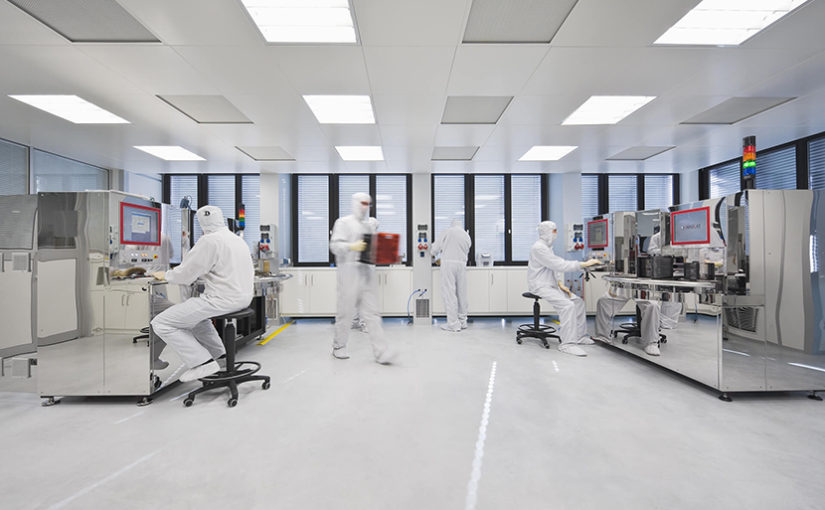
Robotics and automation technologies became critical to semiconductor manufacturing more than a decade ago, especially in 200mm fabs. In fact, cleanroom robotics is said to be the innovation which has enabled the boom in semiconductor manufacturing.
In the past five years, fabs have been moving from 200mm to 300mm, with Intel considering establishing a 450mm fab.
These numbers – 200mm, 300mm and 450mm – refer to the diameter of the silicon wafers, which look like old-fashioned music CDs.
It’s these silicon wafers on which the chips are deposited through a process too complicated to get into in this article.
The nanometer number refers to how small the transistors can be made. The smaller they are, the more precise the manufacturing equipment needs to be.
Some people say semiconductor manufacturing equipment is not precise enough to make transistors smaller than 10 nanometers, or that the silicon itself – the base material for semiconductors – cannot keep transistors apart at such small scales, or that electrons will jump around and not stay within the tiny spaces they are supposed to.
The central, most important space in a typical fab is the cleanroom, which is called a cleanroom because it is thousands of times cleaner than the average room – completely free of dust and other free-floating particles – and is of a controlled temperature and humidity.
Cleanroom equipment
There are many types of equipment required in a typical fab and in the cleanroom and some very hi-tech companies supplying them.
The most important piece of equipment is, arguably, the lithography machine, which sort of prints the circuitry of the chips onto the wafers. It could be likened to 3D printing, but in fact is a very old, optical technology.
A company called Zeiss claims most of the world’s microchips are manufactured using its optical technologies.
Among the many pieces of equipment Zeiss offers is an electron microscope.
Another company which claims to be a world leader in this sector is ASML, which specialises in photolithography systems.
But neither Zeiss nor ASML apparently offer industrial robots, which is probably what readers of this website are more interested in.
Cleanroom robots can be put to work in either an atmospheric cleanroom or in a vacuum.
The type of robots generally found in cleanrooms are SCARA – or Selective Compliance Articulated Robot Arm – robots, delta, or articulated robots, or all three. A variety of other, different shapes and configurations are also to be found in a typical fab.
Mostly they are used to handle the silicon wafers, move them from one position to another, but they can also be used for polishing and inspection. Probably most importantly, they are used for the deposition of conductive materials on the substrate, or wafer.
Here is a random selection of industrial robot companies which offer cleanroom certified robots, and we will be taking a closer look at these in another article.